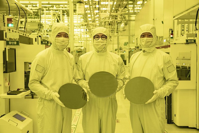
The entry of Samsung into 3-nanometer foundry processor manufacturing kicks off, and the South Korean company will reportedly start producing Gate-All-Around-based chipsets this week, Samsung New3sroom disclosed on Thursday.
The electronics juggernaut is making rapid progress toward finishing the creation of chipsets that could assist the mining of Bitcoin. The company alluded to the new initiative during the first quarter earnings call of 2022.
Suggested Reading | North Korean Hackers Suspected Of Perpetrating $100 Million Harmony Attack
3-Nanometer Chips Can Ease Bitcoin Mining Pain Points
Samsung’s capacity to produce 3-nanometer processors is likely to alleviate some Bitcoin mining difficulties.
In comparison to the 5nm process, the first-generation 3nm technology can cut power usage by up to 45 percent, boost performance by 23 percent, and decrease area size by 16 percent.
The second-generation 3nm technology can only minimize power consumption by around half, increase performance by 30 percent, and minimize area by 35 percent.
FinFET (fin-shaped field-effect transistor), which uses only three surfaces instead of four, has been the most commercially successful technique to date. Reportedly, the company’s latest improvement permits narrower gates and more exact current regulation.

Three-nanometer chipsets are more powerful and efficient. Source: Wccftech
Dr. Siyoung Choi, president and head of Samsung Electronics’ Foundry Business, stated:
“Samsung has grown rapidly as we continue to demonstrate leadership in applying next-generation technologies to manufacturing… We aim to continue this leadership with the world’s first 3nm process with the MBCFET.”
The largest company in South Korea, will reportedly begin trial fabrication of three nanometer (3nm) chips for application-specific integrated circuits (ASICs) — the most efficient equipment for bitcoin mining – this week.
According to sources, the company’s production volume is still low and more of a test run than mainstream production.
Chinese ASIC Company Is Samsung’s First Customer
Reports also have it that Samsung’s first client is the Chinese ASIC manufacturer PanSemi, which designs ASICs used for bitcoin mining.
Qualcomm, Samsung’s biggest customer, had also made reservations for the technology, with the two companies agreeing that Qualcomm can opt in at any time but is not committed, reports said.
BTC total market cap at $374 billion on the daily chart | Source: TradingView.com
Suggested Reading | Three Arrows Capital In Deep Trouble As Court Orders For Its Liquidation
Chipsets Seen To Play Crucial Role In Bitcoin Mining
These chipsets are anticipated to play a vital role in Bitcoin mining, resulting in intense competition among industry leaders to produce novel technologies.
Blockscale is the name of a new bitcoin mining processor that Intel has introduced. Intel added that the chip can produce more energy and efficiency at SHA-256 hashing.
With its soon-to-be-launched product, the South Korean company will compete with Taiwan Semiconductor Manufacturing Company (TSMC), which also produces specialized chips.
Joe Sawicki, executive vice president of Siemens Digital Industries Software’s IC-EDA division, was quoted by Samsung Newsroom as saying:
“Siemens is pleased to have collaborated with Samsung to help ensure that our existing software platforms also work on Samsung’s new 3-nanometer process node since the initial development phase.”
Featured image from Samsung Newsroom, chart from TradingView.com


